


Description
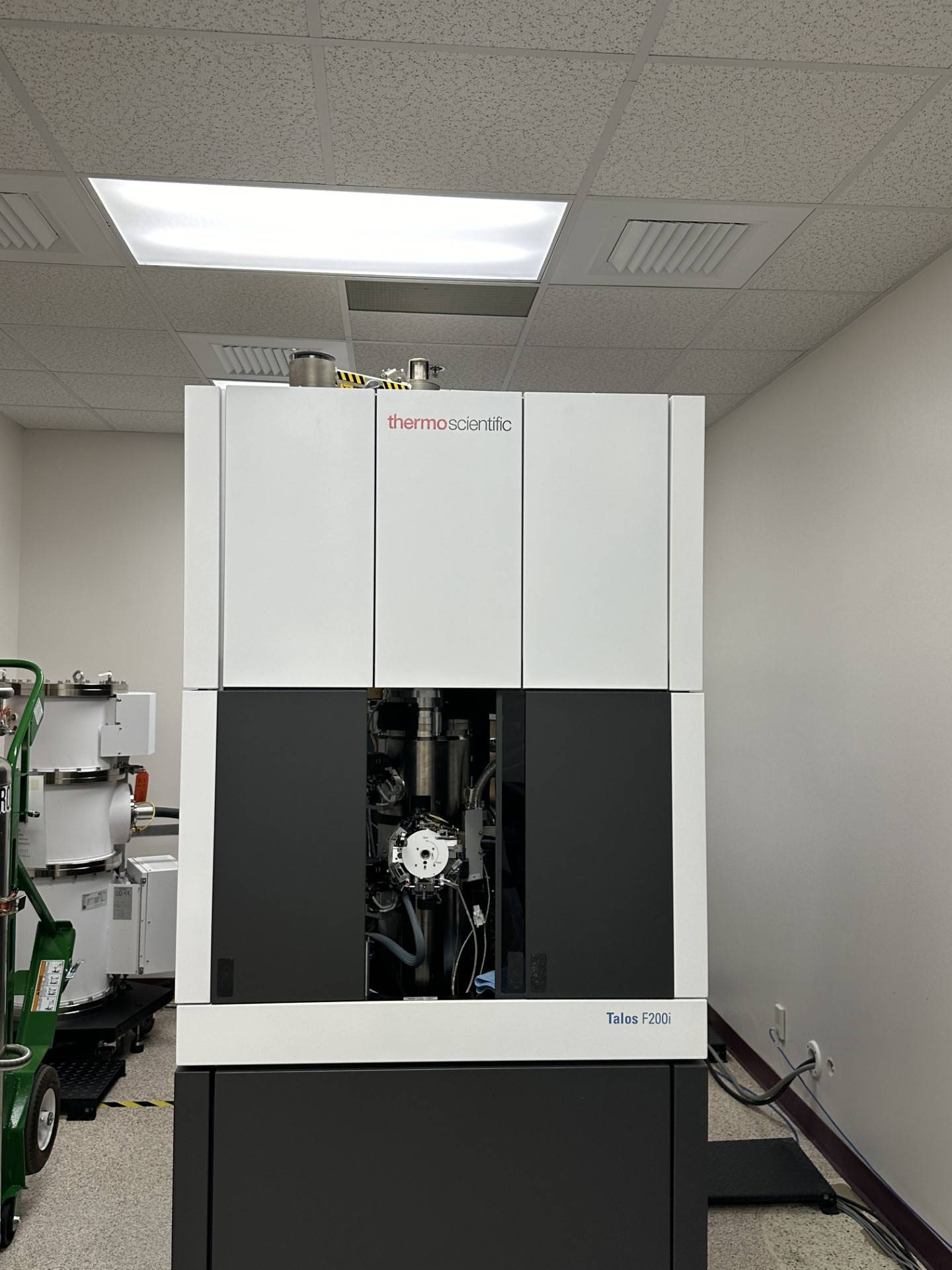
The FEI Talos™ f200i S/TEM is a 200 kV field emission (scanning) transmission electron microscope that has been designed for fast, precise and quantitative characterization of nanomaterials; achieving atomic resolution. With column alignments at 120 kV and 200 kV the Talos™ f200i S/TEM is capable of imaging a broad range of materials science and biological samples.
The S/TEM column is fully automated, equipped with a S-FEG, isolated vacuum system for the electron gun, symmetric X-TWIN objective lens, computerized 5 axes eucentric goniometer, diffraction lens, intermediate lens, two projector lenses, fast survey camera, and a vibration-free vacuum system.
Techniques include: brightfield (BF), darkfield (DF), high resolution-TEM (HR-TEM for crystalline samples), diffraction, selected area electron diffraction (SAED), nanobeam diffraction, convergent beam electron diffraction (CBED), scanning transmission electron microscopy (STEM), high resolution-STEM (HR-STEM), and Energy Dispersive X-Ray Spectroscopy (EDS).
Capabilities
- Accelerating voltage: 120 kV and 200 kV (possible to do 80 kV)
- Magnification Range: 25X – 1.05MX
- TEM line resolution: ≤0.12nm
- STEM resolution: ≤0.16nm
- HAADF STEM detector
- Maximum full convergence angle for LACBED: ≥ 100mrad
- Maximum diffraction angle: 24°
- Z-movement total travel (standard holders): ±0.375mm
- Maximum tilt with double tilt holder: α ± 30°, β ± 30°
- Specimen drift (standard holders): ≤ 0.5nm/min
- 4k x 4k CETA 16M CMOS Camera
- Sample holders
- Single tilt holder
- Double tilt holder
- Low background double tilt HIVis holder
- Maximum tilt with double tilt holder: α ± 35°, β± 30°
- Maximum Diffraction angle: 24°
- 30 mm2 retractable Bruker X-flash™ 6|30 EDS detector
- Velox™ advanced acquisition and processing software
Location: Supple 171
Manager: Dr. Casey Smith, casey.smith@txstate.edu
Trainer: Chironjib Chandan, chironjib.chandan@txstate.edu
Model: FEI TALOS f200i
Funded by: The Materials Applications Research Center (MARC)