Description
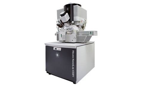
The FEI Helios NanoLab 400 DualBeam system is a fully digital Field Emission Scanning Electron Microscope (FE SEM) equipped with Focused Ion Beam (FIB) technology. The DualBeam platform is used for sample preparation, imaging and analysis in semiconductor failure analysis, process development, and process control laboratories.
Ultra-high resolution electron optics are capable of 0.9 nm at optimal working distance (15 kV) and 1.0 nm at the DualBeam coincident point and 350 V – 30 kV beam voltage range.
The Sidewinder ion column for FIB combines high-resolution with low voltage performance. This enables excellent ion image resolution (5 nm @ 30 kV, coincident WD) with 500V-30kV beam voltage range and precise ion milling. The small beam diameter of the Sidewinder ion column at less than 1 kV enables low-energy, grazing-incidence final clean-up to remove surface damage induced by higher-energy milling.
Capabilities
- Load lock maximum sample size (X-Y-Z): 150mm x 150mm , thickness 8mm
- Weight limitation: 200g if you use load lock and/or Tilt stage. 500g absolute.
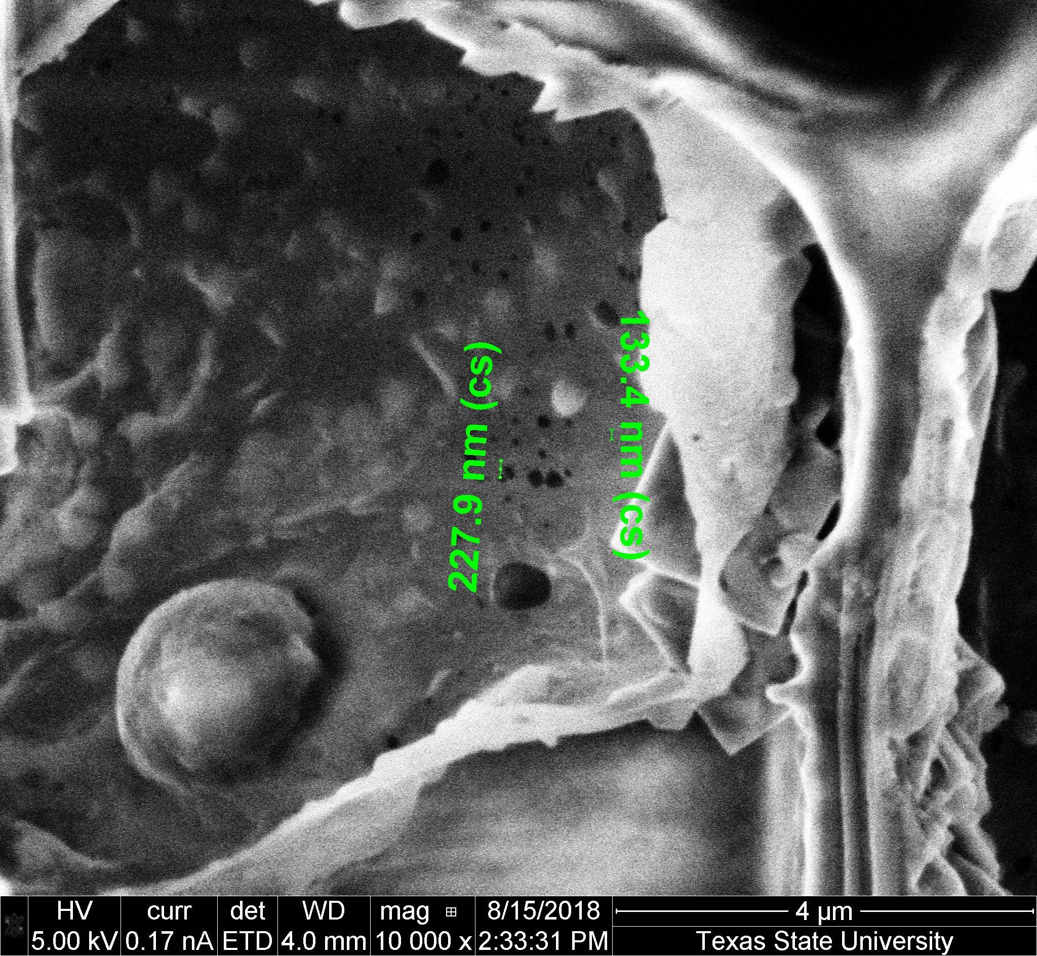
- Demonstrated Resolution: 1.9 nm
- 5-axis motorized x-y-z-rotate-tilt stage with piezo control of all axes
- x and y-axes is 100 mm, the tilt range is -10 to +60 degrees, motorized z range is 20 mm
- Energy dispersive X-ray (EDX) provides elemental analysis
- TEOS deposition source, metalorganic sources for Pt and W
- Gas injection system (GIS)
Which ‘tome’ is right for me?
Click here for a tome tool comparison guide.
Location: RFM1202
Manager: Dr. Joyce Anderson jha39@txstate.edu
Backup: Dr. Casey Smith casey.smith@txstate.edu
Model: Helios Nanolab 400
Donated/funded by:
National Science Foundation - Division Of Materials Research
NSF DMR-0923509 (Program Manager: Guebre X. Tessema). Principal Investigator: Dr. Nikoleta Theodoropoulou; CoPi's: Dr. Thomas Myers, Dr. Jennifer Irvin, Dr. Chang Ji, Dr. Gary Beall.