Mission and Objectives
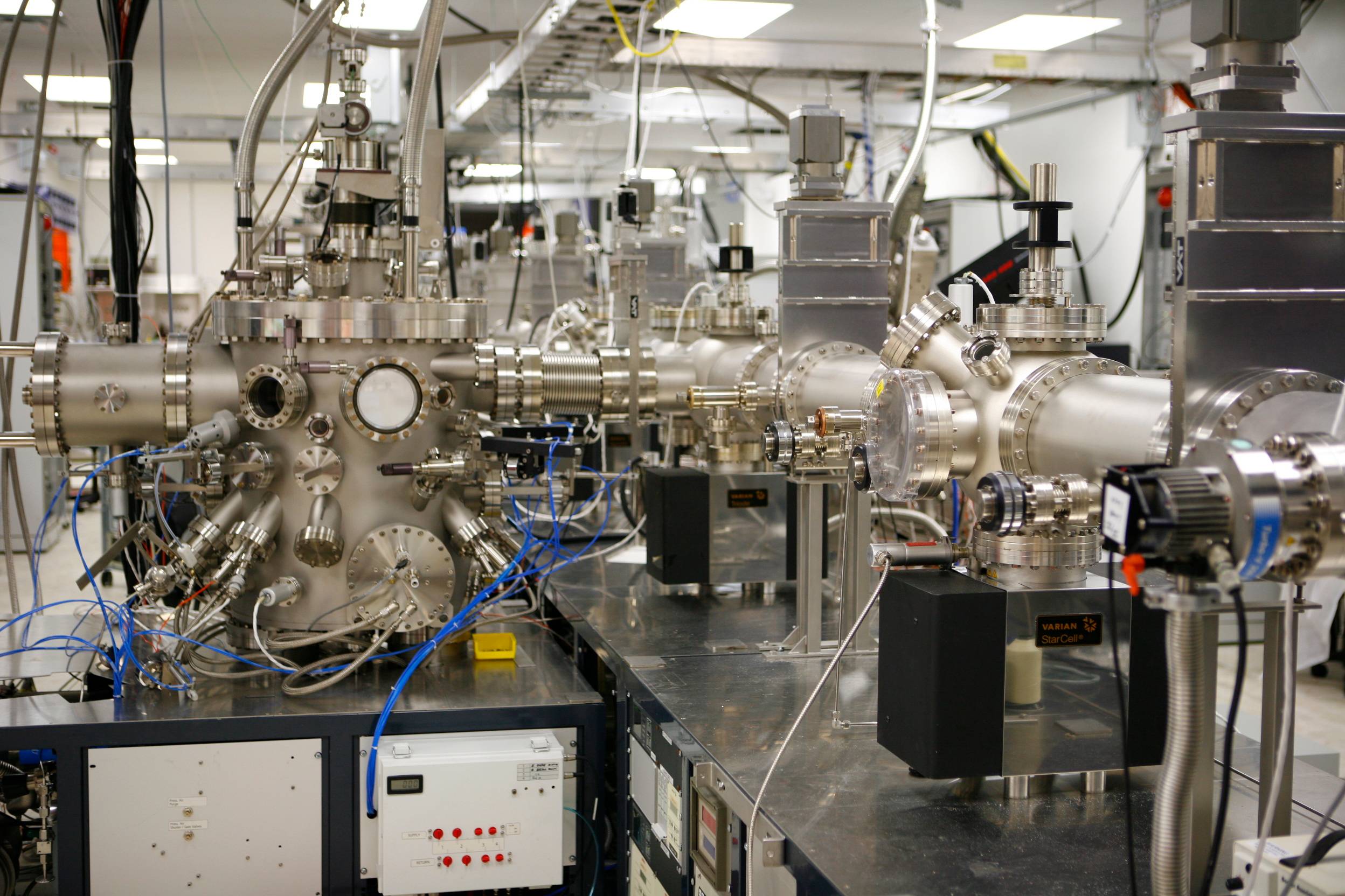
The Epitaxy Research Shared Space (ERSS) is located in the Roy F. Mitte (RFM) building and contains a unique set of equipment all designed to grow crystalline thin films in a process called heteroepitaxy. The two main types of systems utilized to grow these thin films are a high-vacuum Molecular Beam Epitaxy (MBE) multi-chamber cluster and a high-temperature Metalorganic Chemical Vapor Deposition (MOCVD) reactor. These systems are typically segregated by material family to prevent cross-contamination and allow our researchers to experiment with a large portion of the periodic table in search of new functional semiconductor and oxide materials.
Filter Panel
-
Antimonide Chamber
Dedicated to growth of compound semiconductors for high-speed
electronics and optoelectronic device applications. Sources include
Be, In, As, GaTe, Ga, Si, Sb, Al effusion cells. -
Arsenide Chamber
Dedicated to growth of compound semiconductors for high-speed
electronics and optoelectronic device applications. Sources include
Al, Ga, GaP, Be, As, Si, In in effusion cells. -
Contactless Mobility
The LEI 1600 Mobility Measurement System has the capability of measuring various semiconductor transport properties, which include mobility, sheet charge density and sheet resistance via a non-contact measurement method.
-
Crystalline Oxides
Growth of crystalline multifunctional oxides on oxide and semiconductor
substrates as well as Si and Si/Ge heterostructures. Current sources include Mn, Fe, La, Ba, Si, Sr, Bi, Ti, and O2plasma. -
High-k Dielectric
Used for the development of gate dielectrics on compound semiconductors
in the quest for a III-V MOSFET device. This chamber has GaO, InO, Ga, Gd, Si, and O2plasma sources. -
In-Situ X-Ray Photoelectron Spectroscopy (XPS)
X-ray Photoelectron Spectroscopy (XPS) is primarily used to probe the bond configurations of atoms in the top 2-5nm of a thin film specimen. Soft X-ray radiation (from Al and/or Mg sources, need both to distinguish XPS from Auger) is directed at the sample to induce emission of inner shell electrons. Measuring the characteristic kinetic energy of the emitted electrons is used to determine their binding energy and therefore what atom they came from as well as the local bonding scheme.
-
IV-VI Compound Semiconductor
Used for the growth of Pb and Sn-based device structures for
infrared imaging and thermoelectric applications. Current sources include PbTe, SnTe, Te, BiTe, and TlTe effusion cells. This chamber shares a Hydrogen surface cleaning chamber. -
Telluride Chamber
Used for the growth of Te-based device structures for infrared
imaging applications. Current sources include CdAs, Te, Mg, Sb, CdTe, Cd, Zn, and Se effusion cells. This chamber shares a Hydrogen surface cleaning chamber.

