


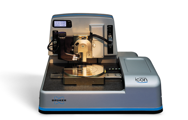
Description
Icon AFM incorporates the latest evolution of Bruker’s nanoscale imaging and characterization technologies on a large sample tip-scanning AFM platform. The Icon’s temperature-compensating position sensors render noise levels in the sub-angstroms range for the Z-axis, and angstroms in X-Y. Number of supported techniques and modules able to map different physical as conductivity, capacitance, piezo response, surface potential, magnetic force, etc. Liquid cell give ability not only make SPM measurement in liquid, but also study electrochemical reactions with AFM probe as one of electrodes.
Ask staff for advanced techniques if interested.
Capabilities
- Maximum Piezo scan size 92μm x 92μm
- Stage Parameters
- Resolution: 1µm
- Repeatability: ±2µm
- Scan range (XY): 154mm X 185mm
- Maximum sample size 8 in, diameter X 0.65 in. thick or 200 mm X 16.5 mm
- Maximum sample weight: 1lb (464 grams)
- Conductive unit (Peak force TUNA) current ranges 20 pA/V to 100nA/V
- AC/DC bias range -10 to +10V
- Modes available:
- KPFM (Kelvin Probe Frequency-modulated)
- SCM (Scanning Capacitance Microscopy)
- QNM (Quantitative Nano-Mechanical)
- PFM (Piezo Response Force Microscopy)
- MFM (Magnetic Force Microscopy)
- SECM (Scanning Electrochemical Microscopy)
- Conductivity mapping
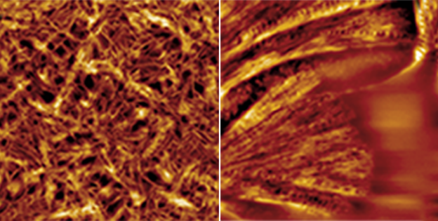
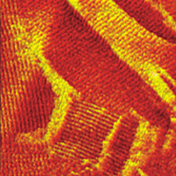
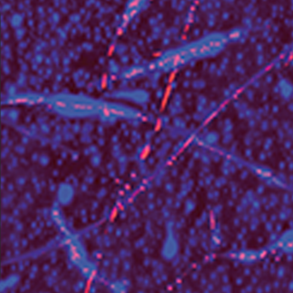
Bruker AFM Example Data
Source: (https://www.bruker.com/en/products-and-solutions/microscopes/materials-afm.html)
Location: RFM1203
Manager: Dr. Joyce Anderson jha39@txstate.edu
Backup: Dr. Casey Smith casey.smith@txstate.edu
Model: Bruker Dimension ICON
Granted by: U.S. Department of Defense AF Office of Scientific Research
W911NF-16-1-0518 (Program Officer Dr. Paul Armistead)